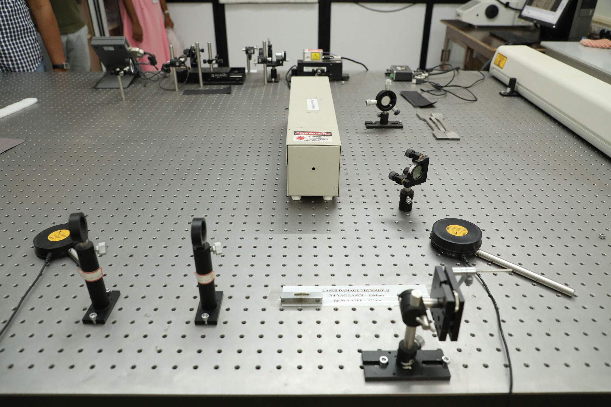
Make: THORLABS
Model: H9307-04
- Measure the optical / radiation limit at which an optical material will be damaged by a laser.
- Laser induced modification or destruction of a material can be measured.
Useful for multiple disciplines of research such as Materials Science and Optical materials.
Room No.: 402
Technology Tower
Centre of Functional Materials
School of Advanced Sciences (SAS)
Dr. S Madeswaran
Centre of Functional Materials
VIT, Vellore, TN-632014.
Email: cfm.ldt@vit.ac.in
Phone:0416- 220 2353/ 58
| User Type | Charges (INR) (+ applicable GST) |
|---|---|
| UG /PG Students from Academic Institution | 423.73 |
| Research Scholar from Academic Institution | 423.73 |
| Project Staff from Academic Institution | 423.73 |
| Faculty Members from Academic Institution | 423.73 |
| Research Scientist from R&D Organizations | 423.73 |
| Industry Personnel from Industry | 423.73 |
| Personnel from Non - Government Organization | 423.73 |
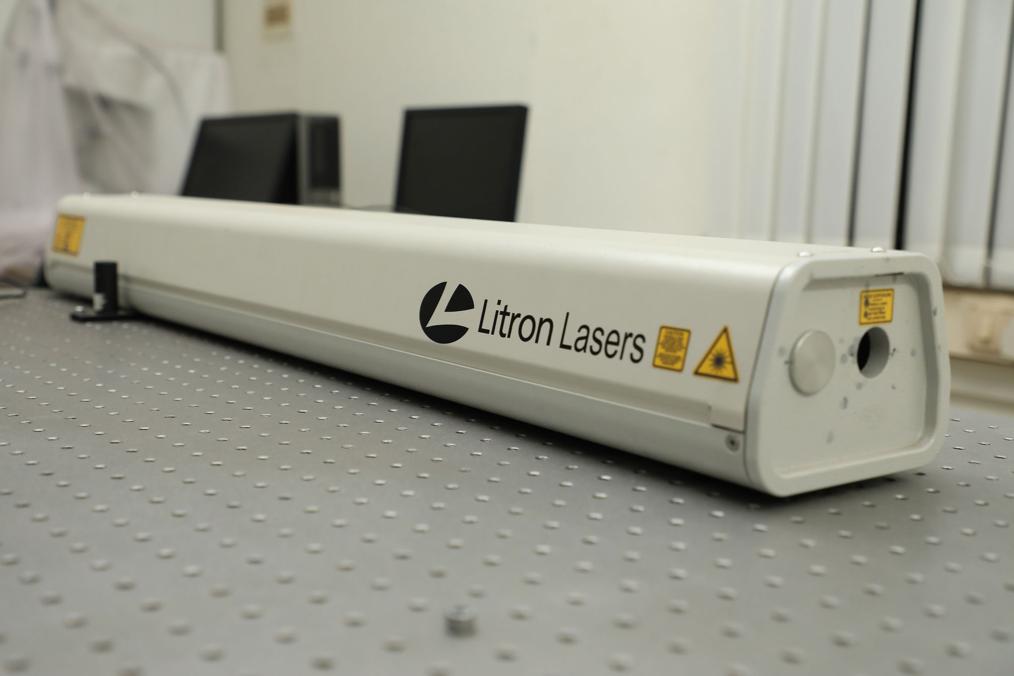
Make: Brand-Litron Lasers
Model: BS EN 60825-1
- Induces Surface Distribution of Residual Stresses
- Increases thermal stability of Residual Stresses
- Induces in-Depth Residual Stress Distribution
- Also be used to strengthen thin sections, harden surfaces, shape or straighten parts and break up hard materials.
Useful for multiple disciplines of research such as Materials Science and Mechanical Engineering
Room No.: 402
Technology Tower
Centre of Functional Materials
School of Advanced Sciences (SAS)
Dr. S Madeswaran
Centre of Functional Materials
VIT, Vellore, TN-632014.
Email: cfm.lsps@vit.ac.in
Phone: 0416-220 2353/58
| User Type | Charges (INR) (+ applicable GST) |
|---|---|
| UG /PG Students from Academic Institution | 847.5 |
| Research Scholar from Academic Institution | 847.5 |
| Project Staff from Academic Institution | 847.5 |
| Faculty Members from Academic Institution | 847.5 |
| Research Scientist from R&D Organizations | 847.5 |
| Industry Personnel from Industry | 847.5 |
| Personnel from Non - Government Organization | 847.5 |
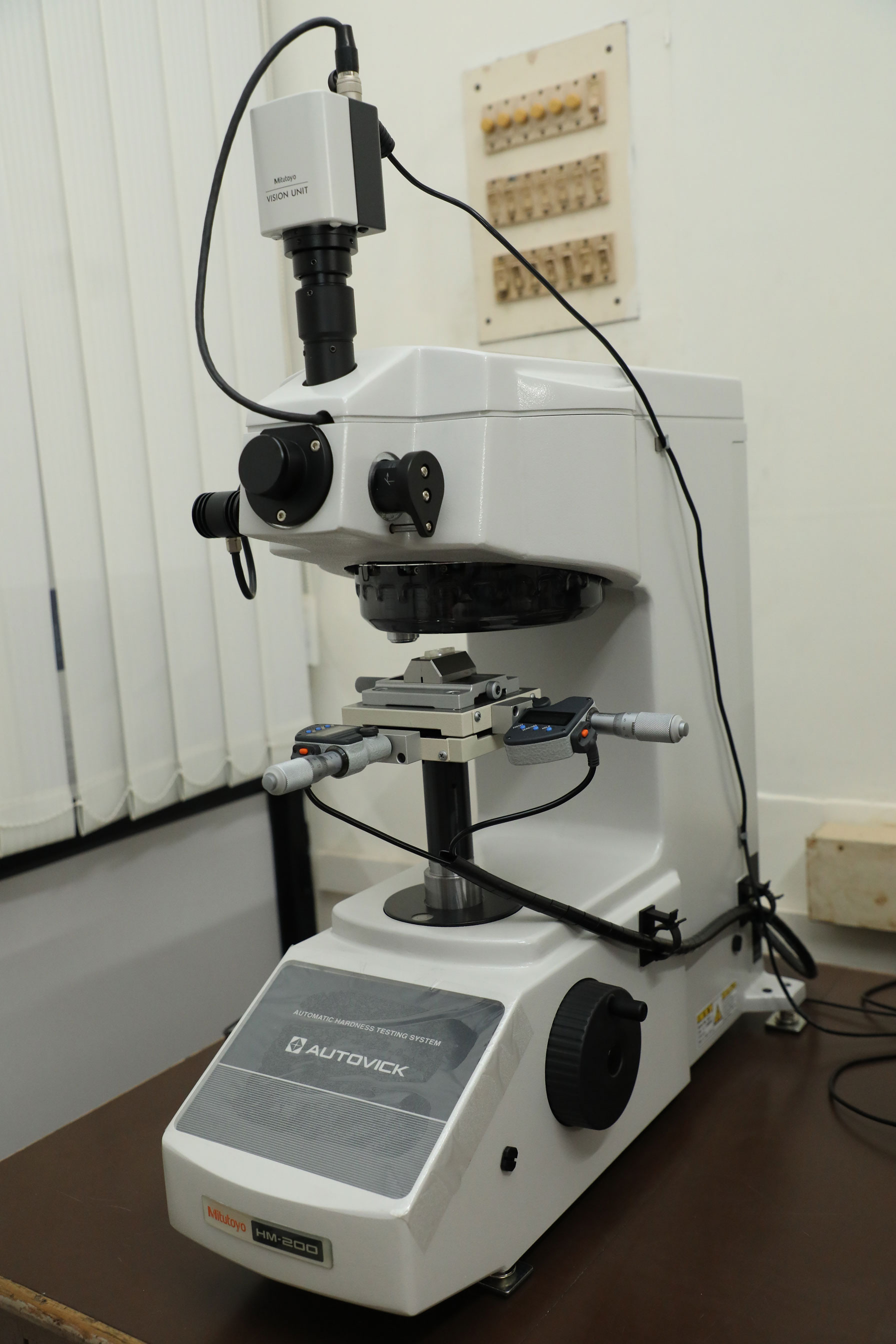
Make: Mitutuoyo
Model: Mitutuoyo-HB210
- Tester vary primarily in load range.
- Accommodate either the vicker's or Knoop Indenters.
- Load from 10 to 1000 gf are directly applied to the top of the indenter.
- For a high-accuracy measurement, the test should be performed on a flat specimen with a polished or prepared surface.
- The quality of the required surface is dependent on the force used.
- In all the tests, the indentation perimeter and depth should be clearly defined when observed by the microscope.
Useful for multiple disciplines of research such as Materials Science, Mechanical engineering, Crystal Growth.
Room No.: 402
Technology Tower
Centre of Functional Materials
School of Advanced Sciences (SAS)
Dr. R EzhilVizhi
Centre of Functional Materials
VIT, Vellore, TN-632014.
Email: cfm.vkhs@vit.ac.in
Phone: 0416- 2202350/53
| User Type | Charges (INR) (+ applicable GST) |
|---|---|
| UG /PG Students from Academic Institution | 500 |
| Research Scholar from Academic Institution | 500 |
| Project Staff from Academic Institution | 500 |
| Faculty Members from Academic Institution | 500 |
| Research Scientist from R&D Organizations | 500 |
| Industry Personnel from Industry | 500 |
| Personnel from Non - Government Organization | 500 |
Make: N/A
Model: N/A
- Measure the nonlinear optical properties of materials.
- Determine intrinsic photo-physical properties of materials by focusing a single laser beams onto the surface of the materials sample.
- Measurements need to be taken at different laser pulse energies or different laser pulse lifetimes in order to determine what nonlinear processes are present.
- Sample (of size 1mm x 1- 10 mm x 1-10 mm) should be flat with a polished surface.
Useful for multiple disciplines of research such as Materials Science, Crystals and Optical materials.
Room No.: 402
Technology Tower
Centre of Functional Materials
School of Advanced Sciences (SAS)
Dr. R EzhilVizhi
Centre of Functional Materials,
VIT, Vellore, TN-632014.
Email: cfm.zst@vit.ac.in
Phone:0416 - 2202350 / 53
| User Type | Charges (INR) (+ applicable GST) |
|---|---|
| UG /PG Students from Academic Institution | 500 |
| Research Scholar from Academic Institution | 500 |
| Project Staff from Academic Institution | 500 |
| Faculty Members from Academic Institution | 500 |
| Research Scientist from R&D Organizations | 500 |
| Industry Personnel from Industry | 500 |
| Personnel from Non - Government Organization | 500 |
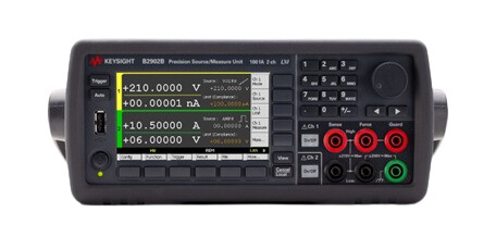
Make: Keysight
Model: B2902B
Voltage range : ±210 V
Current range :±3 A DC, ±10.5A pulsed
Accuracy : 0.015%
Source and measurement
Resolution : 10 fA and 100 nV
Sample Preparation:
• Thin films or pallets with metallic contact pads
• Maximum, sample size 1in x 1in.
- Precise voltage/current source and measurement
- Perform Restivity, I-V Characterization, DC or Pulsed I-V test
- Semiconductor Component Test, Verification, and Analysis
- Two-leaded Diodes, laser diodes, LEDs, Photodetectors, sensors
- Three terminal field effect transistors (FETs), bipolar junction transistors(BJTs)
- Complete Automated System
- Limit (compliance) feature prevents device damage
- Integrated sweep and arbitrary waveform measurement functionality
402 - Technology Tower, CFM Lab
Centre for Functional Materials
Vellore Institute of Technology –Vellore Campus
Thiruvalam Road,Vellore,Tamil Nadu, India.
Assistant Professor
Centre for Functional Materials
TT-431, VIT Vellore Campus,
Katpadi, Vellore, Tamil Nadu 632014
E-mail ID: ankur.rastogi@vit.ac.in
| S. No. | User Type | Charges for per hour in INR |
|---|---|---|
| 1 | Students (UG/PG)/Research Scholars from VIT | 100 |
| 2 | UG /PG Students from Academic Institutions | 200 |
| 3 | Research Scholar from an Academic Institution | 200 |
| 4 | Project Staff from Academic Institutions | 200 |
| 5 | Faculty Members from Academic Institutions | 300 |
| 6 | Research Scientist from R&D Organizations | 500 |
| 7 | Industry Personnel from Industry | 1000 |
| 8 | Personnel from Non - Government Organizations | 1000 |
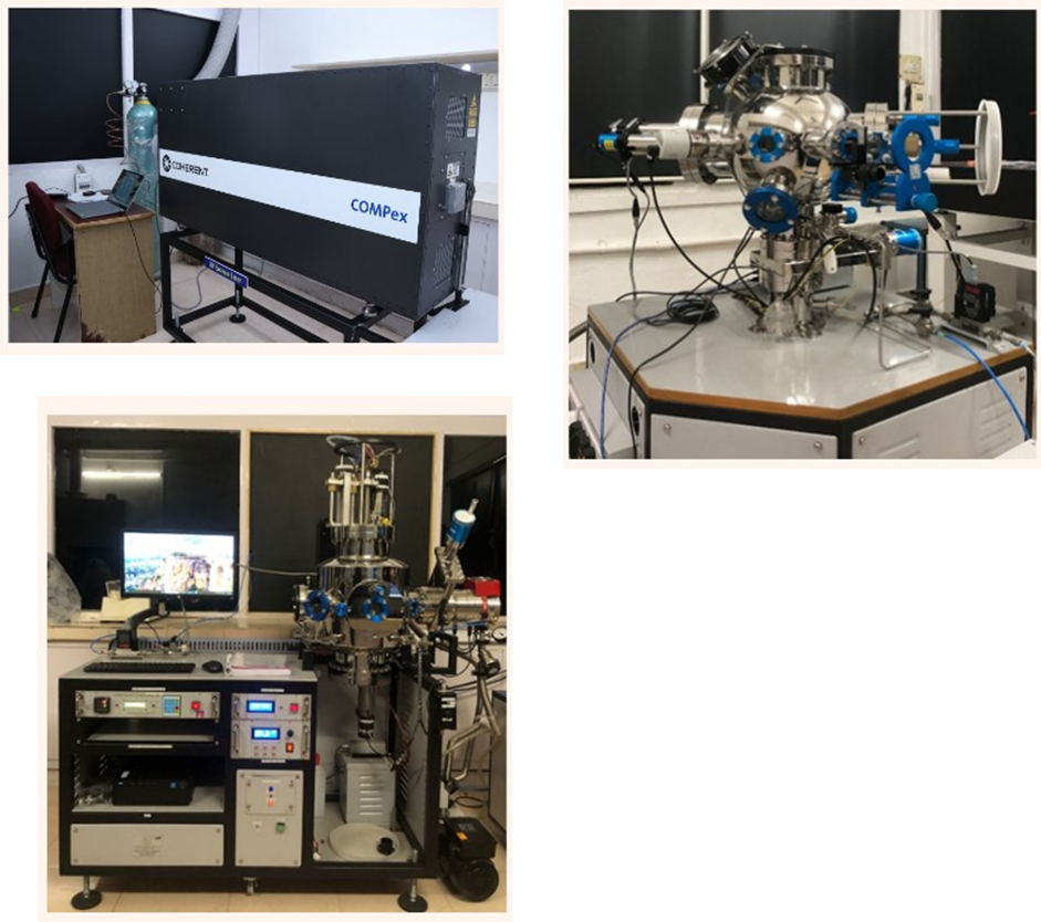
Make: Coherent
Model: COMPex 201 F
Laser System:
Gas : KrF
Wavelength : 248 nm
Maximum Energy : 750 mJ
Pulse duration : 20 ns
Maximum Frequency : 10 Hz
Deposition Chamber:
1. Standard Chamber:
Maximum deposition area: 1 cm x 1 cm
Target size : 1 inch
Targets : 6
Substrate temperature : 800 °C
Target Rastering
Maximum Sample size : 1 cm x 1 cm
2. Large Area Chamber:
Maximum deposition area: 2.5cm x 2.5 cm
Target size : 1 or 2 inch
Substrate temperature: 800 °C
Laser and Target Rastering
Uniformity over 1 square inch
- Pulsed Laser Deposition (PLD) is a PVD technique used to deposit thinfilms of various materials. The PLD process involves directing a high-energy laser beam onto a target, which ablates the atoms of the target material. The ablated particles form vaporised plasma and are then deposited on the substrate.
- A key advantage of PLD is that it yields high-quality stoichiometric thinfilms. It is a versatile technique for depositing multicomponent materials like complex oxides, nitrides, etc. It also allows precise control of the thickness of the film, especially when equipped with in situ units like RHEED.
- PLD-deposited films have broad applications in semiconductors, memory Devices, spintronics, sensors, solar cells, superconductors, etc.
402 - Technology Tower, CFM Lab,
Centre for Functional Materials
Vellore Institute of Technology –Vellore Campus,
Thiruvalam Road,Vellore,Tamil Nadu, India.
Dr. Atul Thakre
Assistant Professor
Centre for Functional Materials
CBMR - 201A, VIT Vellore Campus,
Katpadi, Vellore, Tamil Nadu 632014
Faculty In-charge E-mail ID: atul.thakre@vit.ac.in
Facility E-mail ID: cfm.pld@vit.ac.in
| S. No. | User Type | Charges in INR |
| 1 | Students (UG/PG)/Research Scholars from VIT | 5000 |
| 2 | UG /PG Students from Academic Institutions | 5000 |
| 3 | Research Scholar from an Academic Institution | 5000 |
| 4 | Project Staff from Academic Institutions | 5000 |
| 5 | Faculty Members from Academic Institutions | 5000 |
| 6 | Research Scientist from R&D Organizations | 5000 |
| 7 | Industry Personnel from Industry | 10000 |
| 8 | Personnel from Non - Government Organizations | 7000 |
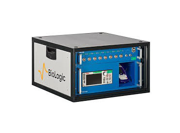
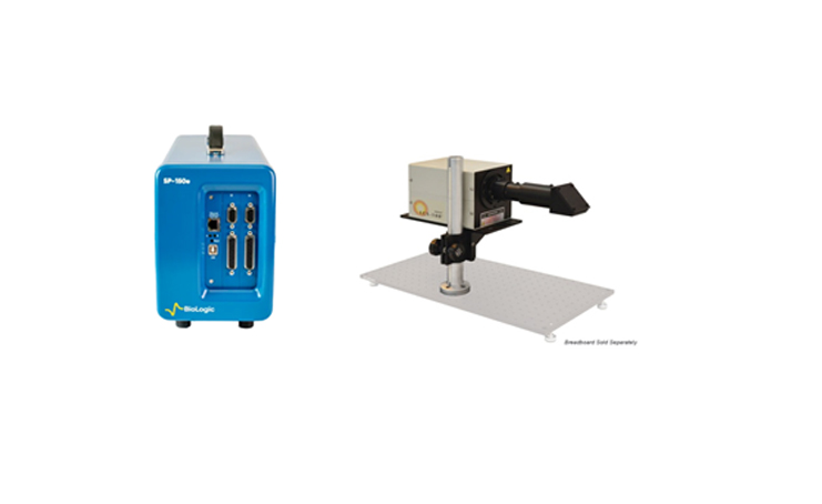
Make: BioLogic
Model: BCS-805
Voltage Range : 0‑10 V, 40 µV resolution, <±0.3 mV accuracy
Current Capability : ±150 mA max, 5 ranges from 100 mA‑10 µA
Current resolution : Down to 0.2 nA, <0.05 % accuracy
EIS Capability : Optional; 10 kHz‑10 mHz, up to 2.5 V & 60 mA amplitude
Sampling Rate : 2 ms acquisition & time base
Analog I/O : 1 (18‑bit) input & 1 (16‑bit) output per module
Cell Connection : 4-terminal + guard
Size & Weight : 1U, ~5 kg
Power Consumption : ~60 W
Cabinet Compatibility : 6U/12U/24U/38U systems available
- Battery Performance Evaluation
- Charge/discharge cycling of single cells and battery packs
- Electrochemical Characterization
- Galvanostatic and potentiostatic control for batteries, supercapacitors, and hybrid devices
- Voltage‑current response characterization
- Rate capability testing
- Material and Electrode Research
- Evaluation of new electrode materials (anodes, cathodes)
- Advanced Diagnostics
- Electrochemical impedance spectroscopy (EIS) for kinetic and transport properties
- Safety and Reliability Testing
- Overcharge/overdischarge tolerance
- High precision current/voltage control for abuse testing
- Thermal effect correlation with electrical performance
- Application Areas
- Lithium-ion, Li‑S, Na-ion, solid-state, and other emerging battery chemistries
- Supercapacitors and hybrid capacitors
- Fuel cell single-cell studies
- Industrial R&D, academic research, and quality control
Device Characterisation Laboratory
Centre for Functional Materials,
Vellore Institute of Technology (VIT), Vellore.
402 Technology Tower
Device Characterisation Laboratory
Centre for Functional Materials (CFM),
Vellore Institute of Technology - Vellore Campus,
Thiruvalam Road, Vellore – 632 014, Tamil Nadu, India.
Office Phone: +91 – 416 – 220 2353
Instrument email ID: cfm.bts@vit.ac.in
| S. No. | Experiment Details | UG /PG Students from Academic Institutions (in INR) | Research Scholar from Academic Institution (in INR) | Project Staff from Academic Institution (in INR) | Faculty Members from Academic Institutions (in INR) | Research Scientist from R&D Organizations (in INR) | Industry Personnel from Industry (in INR) |
|---|---|---|---|---|---|---|---|
| 1 | Battery Test System | 300 | 1000 | 1000 | 1000 | 2500 | 2500 |
* Charges for per sample in INR (+ applicable GST)
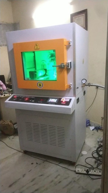
Make: Ants innovation private limited
Model:
Measuring Tc : K type
Control Tc : K type
Maximum Temperature: 1100 C
Working Temperature: 1050 C
Temperature for profiling : 1050 C
Hot Zone(mm): 55X400
- Growth of epitaxial layers (Si, Ge, GaAs, GaN, InP, etc.) with controlled doping and thickness
- Controlled growth of carbon nanotubes (CNTs) and graphene, where catalyst activation and CNT elongation need different zones.
- Nanowires and quantum dots (Si, GaN, ZnO, etc.) with composition gradients or heterostructures
High Temperature lab
Centre for Functional Materials,
Vellore Institute of Technology (VIT), Vellore.
402 Technology Tower
Centre for Functional Materials (CFM),
Vellore Institute of Technology - Vellore Campus,
Thiruvalam Road, Vellore – 632 014, Tamil Nadu, India.
Office Phone: +91 – 416 – 220 2353
Email id: rameshm.thamankar@vit.ac.in
Instrument email ID: cfm.mzcvds@vit.ac.in
| S. No. | Experiment Details | UG /PG Students from Academic Institutions (in INR) | Research Scholar from Academic Institution (in INR) | Project Staff from Academic Institution (in INR) | Faculty Members from Academic Institutions (in INR) | Research Scientist from R&D Organizations (in INR) | Industry Personnel from Industry (in INR) |
|---|---|---|---|---|---|---|---|
| 1 | Multi-Zone Chemical Vapour Deposition (CVD) system | 500 | 1500 | 1500 | 1500 | 3000 | 3000 |
* Charges for per sample in INR (+ applicable GST)
Make: Biologic-SP-150e / NewportLCS-100 94011A
Model:
- Make and Model: Biologic-SP-150e
- Year: 2023
- Voltage: ± 10 V
- Current: ± 10 µA to ± 1 A
- EIS: 1 MHz to 10 µHz
- Make and Model: NewportLCS‑100 94011A
- Source: 100 W xenon lamp
- One sun illumination withAM 1.5G Filter
- Class ABB spectral match
- Material Characterization, Battery and Supercapacitor Testing, Corrosion Studies
- Hydrogen Evolution Reaction (HER), Oxygen Evolution Reaction (OER), and Oxygen Reduction Reaction (ORR)
Centre for Functional Materials,
Vellore Institute of Technology (VIT), Vellore.
Professor
Centre for Functional Materials
TT-408, VIT Vellore Campus,
Katpadi, Vellore, Tamil Nadu 632014
Email id: rezhilvizhi@vit.ac.inContact
Instrument email ID: cfm.ecwss@vit.ac.in
| S. No. | Experiment Details | Students (UG/PG)/Research Scholars from VIT | UG /PG Students from Academic Institutions (in INR) | Research Scholar from Academic Institution (in INR) | Project Staff from Academic Institution (in INR) | Faculty Members from Academic Institutions (in INR) | Research Scientist from R&D Organizations (in INR) | Industry Personnel from Industry (in INR) |
|---|---|---|---|---|---|---|---|---|
| 1 | Electrochemical workstation | 1100 | 1700 | 1700 | 1700 | 1700 | 4500 | 4500 |
| Electrochemical workstation with solar stimulator | 3000 | 4000 | 4000 | 4000 | 5000 | 7000 | 7000 |
* 4 hours per slot
*Platinum electrode, Reference electrode should be bring by your own
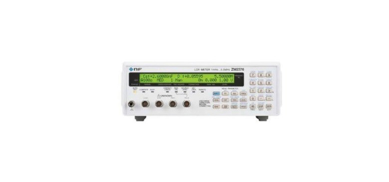
Make: NF Corporation Japan
Model: ZM2378
Basic accuracy : 0.08%.
Measurement signal : 10 mVrms ‑ 5 Vrms, 1 µArms ‑ 200 mArms.
DC bias : Internal 0‑2.5 V or 0‑5.0 V
Measurement time / speed : High-speed modes,typical ≈2 ms
Measured parameters : |Z|, |Y|, L, C, R, G (plus Q, D, θ, X, B, Rs, Rp
- Precise measurement of passive components under controlled temperature.
- Helps in characterizing behaviour across a wide temperature range.
- Evaluates how dielectric, magnetic, and conductive properties vary with temperature.
- Essential for materials used in harsh or varying environmental conditions.
Ceramic composites Laboratory,
Centre for Functional Materials,
Vellore Institute of Technology (VIT), Vellore.
505- Technology Tower
Ceramic composites Laboratory,
Centre for Functional Materials (CFM),
Vellore Institute of Technology - Vellore Campus,
Thiruvalam Road, Vellore – 632 014, Tamil Nadu, India.
Office Phone: +91 – 416 – 220 2353
Instrument email ID: cfm.lcr@vit.ac.in
| S. No. | Experiment Details | Students (UG/PG)/Research Scholars from VIT | UG /PG Students from Academic Institutions (in INR) | Research Scholar from Academic Institution (in INR) | Project Staff from Academic Institution (in INR) | Faculty Members from Academic Institutions (in INR) | Research Scientist from R&D Organizations (in INR) | Industry Personnel from Industry (in INR) |
|---|---|---|---|---|---|---|---|---|
| 1 | Electrospining machine | 300 | 500 | 500 | 500 | 700 | 1000 | 1000 |
* Charges for per sample in INR (+ applicable GST)
Make: NF Corporation Japan
Model: ZM2378
Basic accuracy : 0.08%.
Measurement signal : 10 mVrms – 5 Vrms, 1 µArms – 200 mArms.
DC bias : Internal 0–2.5 V or 0–5.0 V
Measurement time / speed : typical ≈2 ms(1kHz-1MHz) or 10ms(120Hz)
Measured parameters : |Z|, |Y|, L, C, R, G (plus Q, D, θ, X, B, Rs, Rp.
Interfaces / options : USB, RS-232; GPIB / LAN
- Precise measurement of passive components under controlled temperature.
- Helps in characterizing behaviour across a wide temperature range.
- Evaluates how dielectric, magnetic, and conductive properties vary with temperature.
- Essential for materials used in harsh or varying environmental conditions
Ceramic composites Laboratory,
Centre for Functional Materials,
Vellore Institute of Technology (VIT), Vellore.
505- Technology Tower
Ceramic composites Laboratory,
Centre for Functional Materials (CFM),
Vellore Institute of Technology - Vellore Campus,
Thiruvalam Road, Vellore – 632 014, Tamil Nadu, India.
Office Phone: +91 – 416 – 220 2353
Instrument email ID: cfm.lcrmtc@vit.ac.in
| S. No. | Experiment Details | UG /PG Students from Academic Institutions (in INR) | Research Scholar from Academic Institution (in INR) | Project Staff from Academic Institution (in INR) | Faculty Members from Academic Institutions (in INR) | Research Scientist from R&D Organizations (in INR) | Industry Personnel from Industry (in INR) |
|---|---|---|---|---|---|---|---|
| 1 | Measurement at Room Temperature for 4 Parameters | 200 | 500 | 2000 | 2000 | 2000 | 2000 |
| 2 | Temperature Below ?200° C for 4 Parameters | 300 | 600 | 2100 | 2100 | 2100 | 2100 |
| 3 | Temperature Below ?600°C for 4 Parameters | 1000 | 2000 | 4000 | 4000 | 4000 | 4000 |
* Charges for per sample in INR (+ applicable GST)
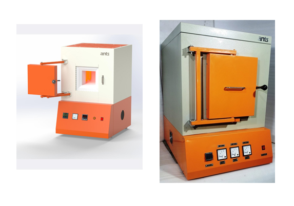
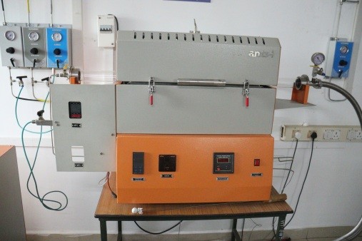
Make: Ants innovation private limited
Model:
Maximum Temperature: 1700 C
Working Temperature: 1600 C
Hot Zone(mm):55X400
- Heat treatment of metals (annealing, tempering, stress relieving).
- Hardening or softening materials for microstructure studies.
- Sintering of ceramics, powders, and composite materials.
- Melting and refining of small metal samples.
- Calibration and testing of thermocouples and sensors.
- High-temperature reaction studies.
- Controlled oxidation/reduction experiments.
High Temperature lab
Centre for Functional Materials,
Vellore Institute of Technology (VIT), Vellore.
402 Technology Tower
Centre for Functional Materials (CFM),
Vellore Institute of Technology - Vellore Campus,
Thiruvalam Road, Vellore – 632 014, Tamil Nadu, India.
Office Phone: +91 – 416 – 220 2353
Email id: rameshm.thamankar@vit.ac.in
Instrument email ID: cfm.muffle@vit.ac.in
| S. No. | Experiment Details | UG /PG Students from Academic Institutions (in INR) | Research Scholar from Academic Institution (in INR) | Project Staff from Academic Institution (in INR) | Faculty Members from Academic Institutions (in INR) | Research Scientist from R&D Organizations (in INR) | Industry Personnel from Industry (in INR) |
|---|---|---|---|---|---|---|---|
| 1 | Muffle Furnace (12 hours per slot) | 500 | 1500 | 1500 | 1500 | 3000 | 3000 |
* Charges for per sample in INR (+ applicable GST)
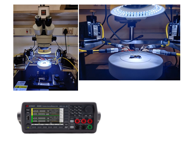
Make: EverBeing Int'l;
Model: C4HT / Keysight B2902B
- Make: EverBeing Int'l;
- Model: C4HT
- Micropositioners :4 probes with magnetic-lock-based
- Probe:Tungsten tips of 5µm diameter
- Temperatures: RT - 200°C(Heatable vacuum chuck)
- Optical microscope: Magnification: 150x;
- Camera: Moticam 8MP
- Model:Keysight B2902B
- Voltage range: ±210 V
- Current range:±3 A DC, ±10.5A pulsed
- Accuracy: 0.015%
- Source and measurement
- Resolution : 10 fA and 100 nV
Measuring I–V, C–V, and resistance on wafers, dies, or packaged devices.
RF / High-Frequency Measurements
With RF probes, supports S-parameter, impedance, and signal Integrity tests.
Temperature-Dependent Testing
With hot chuck (up to ~200 °C), enables study of device behavior vs. temperature.
Low-Noise / Shielded Measurements
Optional shielding boxes allow probing of ultra-low Current/voltage devices.
Device Characterisation Laboratory
Centre for Functional Materials,
Vellore Institute of Technology (VIT), Vellore.
402 Technology Tower
Device Characterisation Laboratory
Centre for Functional Materials (CFM),
Vellore Institute of Technology - Vellore Campus,
Thiruvalam Road, Vellore – 632 014, Tamil Nadu, India.
Office Phone: +91 – 416 – 220 2353
Instrument email ID: cfm.pssmu@vit.ac.in
| S. No. | Experiment Details | UG /PG Students from Academic Institutions (in INR) | Research Scholar from Academic Institution (in INR) | Project Staff from Academic Institution (in INR) | Faculty Members from Academic Institutions (in INR) | Research Scientist from R&D Organizations (in INR) | Industry Personnel from Industry (in INR) |
|---|---|---|---|---|---|---|---|
| 1 | Probe Station with Source Meter Unit | 1000 | 1000 | 1000 | 1000 | 2000 | 2000 |
* Charges for per sample in INR (+ applicable GST)
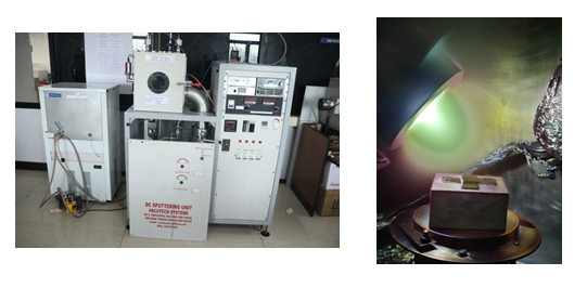
Make: Vacutech System
Model:
Chamber Volume: Approx.. 70 L
RF Power: Max 300W with attached auto tuner
DC power: Max 1000 V
Substrate Heater: Max 300°C
- Gold (Au), Silver (Ag), Copper (Cu), Aluminum (Al), and Tungsten (W) coatings.
Reflective & Decorative Coatings:
- Mirror coatings (Al, Ag) for optics, solar panels, and decorative hardware.
- SiO2, Al2O3, HfO2, TiO2 for capacitors, MOS devices, and passivation layers.
- ZnO, CdS, Ga2O3, and other oxide semiconductors for photovoltaics and sensors.
High Temperature lab
Centre for Functional Materials,
Vellore Institute of Technology (VIT), Vellore.
402 Technology Tower
Centre for Functional Materials (CFM),
Vellore Institute of Technology - Vellore Campus,
Thiruvalam Road, Vellore – 632 014, Tamil Nadu, India.
Office Phone: +91 – 416 – 220 2353
Email id: rameshm.thamankar@vit.ac.in
Instrument email ID: cfm.dcrf@vit.ac.in
| S. No. | Experiment Details | UG /PG Students from Academic Institutions (in INR) | Research Scholar from Academic Institution (in INR) | Project Staff from Academic Institution (in INR) | Faculty Members from Academic Institutions (in INR) | Research Scientist from R&D Organizations (in INR) | Industry Personnel from Industry (in INR) |
|---|---|---|---|---|---|---|---|
| 1 | DC & RF Magnetron Sputtering (5 hours per slot) | 500 | 1500 | 1500 | 1500 | 1500 | 3000 |
* Charges for per sample in INR (+ applicable GST)
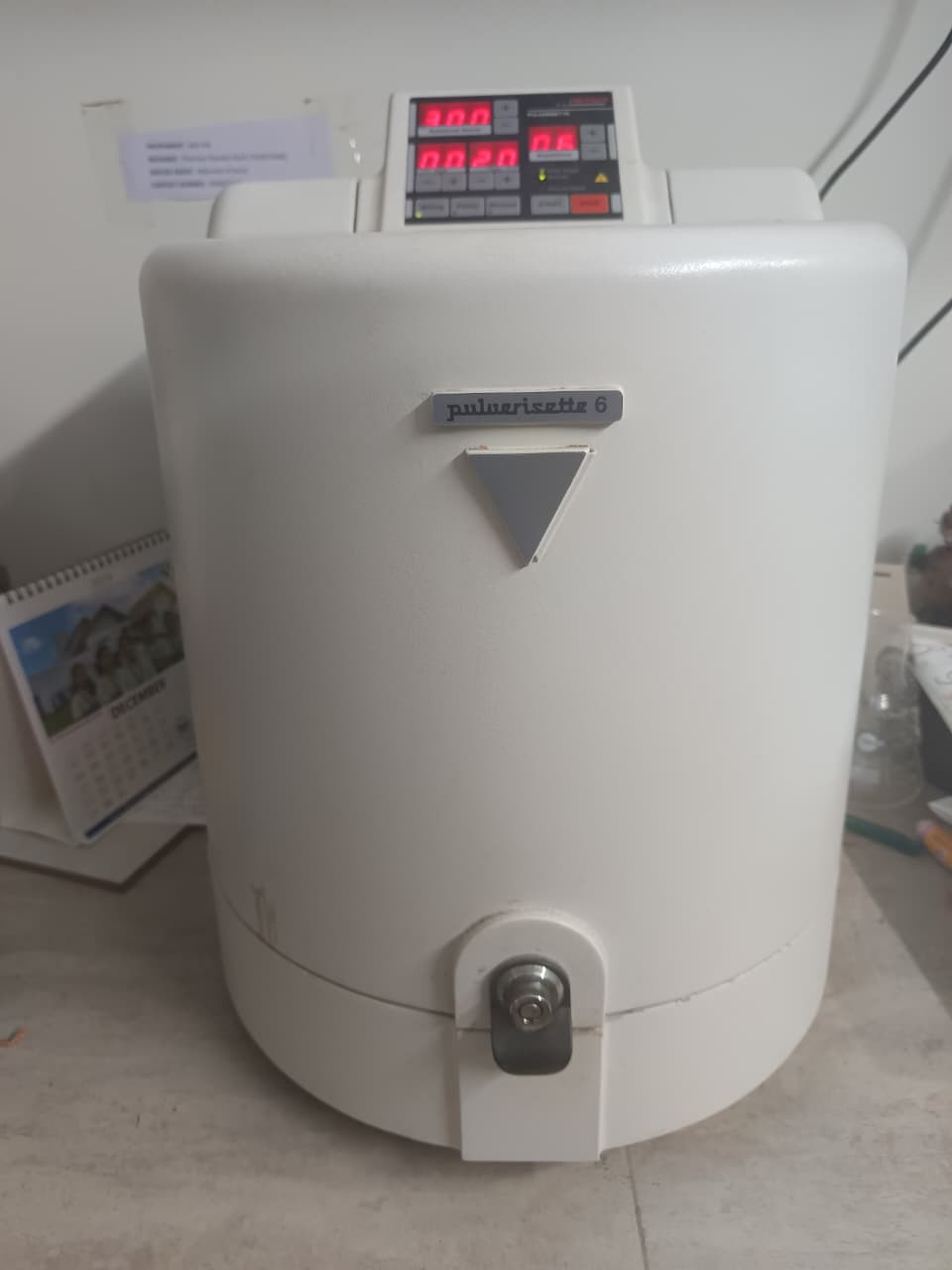
Make: FRITSCH
Model: 03964
Grinding bowl sizes available: 500, 250, 80, 45, 12 ml (various bowl materials)
Grinding ball diameters : 0.1 mm – 40 mm;
Final fineness can reach :< 1 µm (material-dependent).
Max. Feed size : ≈ 10 mm (depends on material).
Sample / charge quantity : 0.5 – 225 ml.
Electrical requirements : 100–120 / 200–240 V single-phase, 50–60 Hz, ~1000 W
Weight & dimensions (approx.): ~63–67 kg; bench-top 370 × 530 × 500 mm
Sound emission : up to ~85 dB (A) depending on load and media.
Modes : dry / wet grinding
- For X-ray fluorescence (XRF), X-ray diffraction (XRD), atomic absorption (AAS), ICP, and other analytical methods.
- Producing homogeneous powder mixtures.
- Solid-state reactions, phase transformations, and amorphization.
- Used in research on nanomaterial’s and advanced alloys.
- To submicron and manometer range (< 1 µm).
- Suitable for dry or wet grinding.
Ceramic composites Laboratory,
Centre for Functional Materials,
Vellore Institute of Technology (VIT), Vellore.
505- Technology Tower
Ceramic composites Laboratory,
Centre for Functional Materials (CFM),
Vellore Institute of Technology - Vellore Campus,
Thiruvalam Road, Vellore – 632 014, Tamil Nadu, India.
Office Phone: +91 – 416 – 220 2353
Instrument email ID: cfm.pm@vit.ac.in
| S. No. | Experiment Details | UG /PG Students from Academic Institutions (in INR) | Research Scholar from Academic Institution (in INR) | Project Staff from Academic Institution (in INR) | Faculty Members from Academic Institutions (in INR) | Research Scientist from R&D Organizations (in INR) | Industry Personnel from Industry (in INR) |
|---|---|---|---|---|---|---|---|
| 1 |
PLANETARY MONOMILL ≥ 3hours to 6hours |
1000 | 1000 | 1000 | 1000 | 2000 | 2000 |
| 2 | ≥ 6hours to 12hours | 1500 | 1500 | 1500 | 1500 | 3000 | 3000 |
| 3 | For every extra 1 hours | 300 | 300 | 300 | 300 | 500 | 500 |
* Charges for per sample in INR (+ applicable GST)