
Make: Thermo Fisher
Model: FEI QUANTA 250 FEG
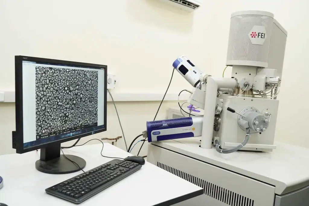
- Capabilities
Capabilities: SEM
- The ability to examine smaller-area contamination spots at electron accelerating voltages compatible with energy dispersive spectroscopy (EDS).
- Reduced penetration of low-kinetic-energy electrons probes closer to the immediate material surface
- To analyse material surfaces at high resolution, including medicine, nanotechnology, materials science, archaeology, and engineering. SEM provides high-resolution images of surface topography and can also determine a material’s chemical composition using energy-dispersive X-ray spectroscopy (EDS).
Capabilities: EBSD
- Microstructure Characterization
- Phase Identification and Mapping
- Deformation and Strain Analysis
- Texture and Anisotropy Studies
- Grain Boundary Engineering
- Additive Manufacturing and Welding Research
- Phase Transformation Studies
- Correlative Microscopy
- Applications
Useful for Nanotechnology, Material Science, Biology, Microstructural Imaging, Compositional analysis of materials, Texture and crystallography of materials
- Charges
For Internal
For External
| EQUIPMENT_NAME | UG /PG Students(in INR) | Research Scholar (in INR) | Faculty Members/ Project Staff (in INR) |
|---|---|---|---|
| FIELD EMISSION SCANNING ELECTRON MICROSOCPE – IMAGING (ONLY FOR METALS) | 500 | 500 | 500 |
| FIELD EMISSION SCANNING ELECTRON MICROSOCPE – IMAGING WITH SPUTTER COATING | 600 | 600 | 600 |
| FIELD EMISSION SCANNING ELECTRON MICROSOCPE – IMAGING + EDX (ONLY FOR METALS) | 600 | 600 | 600 |
| FIELD EMISSION SCANNING ELECTRON MICROSOCPE – IMAGING + EDX WITH SPUTTER COATING | 700 | 700 | 700 |
| FIELD EMISSION SCANNING ELECTRON MICROSOCPE – IMAGING + EDX + MAPPING (ONLY FOR METALS) | 800 | 800 | 800 |
| FIELD EMISSION SCANNING ELECTRON MICROSOCPE – IMAGING + EDX + MAPPING WITH SPUTTER COATING | 900 | 900 | 900 |
| FIELD EMISSION SCANNING ELECTRON MICROSOCPE – EBSD ANALYSIS PER HOUR (ONLY FOR METALS) | 1500 | 1500 | 1500 |
For External
| EQUIPMENT_NAME | UG /PG Students from Academic Institution (in INR) | Research Scholar from Academic Institution (in INR) | Project Staff from Academic Institution (in INR) | Faculty Members from Academic Institution (in INR) | Research Scientist from R&D Organizations (in INR) | Industry Personnel from Industry (in INR) | Personnel from Non – Government Organization (in INR) |
|---|---|---|---|---|---|---|---|
| FIELD EMISSION SCANNING ELECTRON MICROSOCPE – IMAGING (ONLY FOR METALS) | 1000 | 1000 | 1000 | 1000 | 1500 | 2000 | 2000 |
| FIELD EMISSION SCANNING ELECTRON MICROSOCPE – IMAGING WITH SPUTTER COATING | 1200 | 1200 | 1200 | 1200 | 1800 | 2400 | 2400 |
| FIELD EMISSION SCANNING ELECTRON MICROSOCPE – IMAGING + EDX (ONLY FOR METALS) | 1200 | 1200 | 1200 | 1200 | 1800 | 2400 | 2400 |
| FIELD EMISSION SCANNING ELECTRON MICROSOCPE – IMAGING + EDX WITH SPUTTER COATING | 1400 | 1400 | 1400 | 1400 | 2100 | 2800 | 2800 |
| FIELD EMISSION SCANNING ELECTRON MICROSOCPE – IMAGING + EDX + MAPPING (ONLY FOR METALS) | 1600 | 1600 | 1600 | 1600 | 2400 | 3200 | 3200 |
| FIELD EMISSION SCANNING ELECTRON MICROSOCPE – IMAGING + EDX + MAPPING WITH SPUTTER COATING | 1800 | 1800 | 1800 | 1800 | 2700 | 3600 | 3600 |
| FIELD EMISSION SCANNING ELECTRON MICROSOCPE – EBSD ANALYSIS PER HOUR (ONLY FOR METALS) | 2500 | 2500 | 2500 | 2500 | 4000 | 4000 | 4000 |
- Location
Room no.: CDMM G10 Ground floor, Electron Microscopy Lab
Center for Materials Characterization and Testing (CMCT).
- Contact
Dr. Srinivasan Narayanan
In-charge of FE-SEM and EBSD
Faculty of School of Mechanical Engineering
VIT Vellore, 632014.
Email: srinivasan.narayanan@vit.ac.in
Instrument Email: fesem@vit.ac.in
Phone: 0416-2202294